PCB Stack-up selection for RF & HSD applications
- kgideacircle
- Apr 27, 2023
- 4 min read
Updated: Jul 12, 2023
PCB stack-ups for High Speed Digital (HSD) and RF applications need a bit more thought than just the number of layers needed to route the circuits.
For instance, constraints on impedance control and insertion loss call for specific type of dielectric materials to be used and not just the copper layers. Furthermore, depending on the application even copper roughness becomes relevant at higher frequencies so choosing the right type of copper becomes critical.
To top it all, there are applications that require asymmetric stack-ups which brings a different set of challenges in terms of layer pressings and pressing order. Provided below are some basic guidelines that will help choose the right stack-up for your RF and HSD application.
Choosing the right RF PCB Stack-up
Step 1: Estimate layers
First, estimate / identify the number of layers needed to route the design. This involves a bit of a guesstimating and experience. It also helps map out how many critical tracking layers with controlled impedance requirements are needed. Sometimes, a feasibility study might have to be carried out to "see" how the circuits and traces flow (especially in HSD designs) in order to come up with a estimated number of layers needed.
Step 2: Figure out drills
Once we roughly know how many layers are needed, we need to understand what type of drills would be required. For example, High speed digital and RF designs would call for buried & blind vias. These can be mechanically drilled or laser drilled. They could be left unfilled or filled with resin and capped or even fully filled with copper, which is generally the case with microvias.
Some applications will require microvia stacking but this introduces a different set of challenges in PCB manufacturing and also in reliability performance of the PCB, so the number of stacked microvias needed has to be carefully considered.
The blind and buried vias define how many press cycles are needed for the PCB to be manufactured, and more press cycles generally equate to less overall yield so the blind and buried vias don’t come for free.

Figure: 3D view of a PCB stack-up.
Image courtesy of Altium. Refer to links at the end for more details
Step 3: Work out trace characteristics
Once the drills are defined, next step is to understand what dielectric thickness are needed – mainly around the impedance controlled layers. Engineers use impedance calculation tools from Polar Instruments or even simulate traces on a 3D EM simulator to precisely understand what dielectric thicknesses, dielectric constant, loss tangent & trace dimensions are needed to meet certain impedance and loss requirements.
Step 4: Choose materials
Once you know what sort of dielectric thickness and dielectric constant (Dk) are required, you could then discuss with a PCB manufacturer to understand the closest available option. You might want to choose something that is mainstream and not a bespoke material – unless your application demands.
Dielectrics generally come in two variants – core & prepreg. Cores are effectively made of one or more prepregs and are considered more stable as they come cured. The prepregs however are cured during the lamination process thereby changes to overall thickness (and hence the Dk) is more likely.
This change in thickness of a prepreg after pressing the layers is referred as pressed thickness. This is critical as impedance calculations typically need to be carried out with pressed thickness. Pressed thicknesses can be obtained from the factory if they have processed this material in the past. Or else, there is a bit of guessing involved.
When using microvias, there is a material trade-off to consider. Microvias are typically laser drilled and can generally be up to 100um depth. So, the chosen dielectric needs to be thinner than 100um.
Step 5: Pay attention to glass weaves
For impedance-controlled layers, engineers tend to choose cores as it provides consistent Dk. Especially if the traces are routed as a microstrip line. The prepregs, as mentioned before, lose some resin when pressed and result in a non-uniform (relatively speaking) dielectric constant (Dk).
This brings us to an important point about fibreglass weaves. Not all dielectric materials are the same even if they have very similar dielectric constant. They all employ different types of glass weaves and resin content which results in a non-uniform fibreglass and resin distribution.
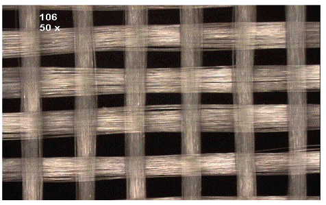

Figure: 106 Glass weave (Left), 2116 Glass weave (Right).
Image courtesy of Isola Group. Refer to links at the end for more details
At RF and HSD frequencies, this weave does play a part in impedance control creating impedance mismatches, so choosing the right weave is also critical.
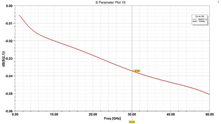
Step 6: Don't ignore copper roughness
And finally, the copper roughness. The rougher the copper the more lossy it is at very high frequencies. RF designs tend to be more sensitive to rougher copper than relatively robust digital designs but at very high speeds, digital has the same challenges as analog / RF !

Figure: Copper roughness and its impact on high frequencies.
Image courtesy of Intel. Refer to links at the end for more details
Once all of the items are understood and defined, its time to have one final discussion with the PCB manufacturer to make sure they have the capability to manufacture your stack-up.
Links:
PCB Stack-up definition in Altium : https://www.altium.com/documentation/altium-designer/blind-buried-micro-vias
Glass weave information : https://www.isola-group.com/wp-content/uploads/Understanding-Glass-Fabric.pdf
Copper Roughness information : https://www.intel.com/content/www/us/en/docs/programmable/683624/current/copper-surface-roughness.html